Visualization of quantum tunneling circuit.[/caption] The powerful, reliable combination of transistors and semiconductors in computer processors could give way to systems built on the way electrons misbehave, all of it contained in circuits that warp even the most basic rules of physics. Rather than relying on a predictable flow of electrons that appear to know whether they are particles or waves, the new approach depends on quantum tunneling, in which electrons given the right incentive can travel faster than light, appear to arrive at a new location before having left the old one, and pass straight through barriers that should be able to hold them back. Quantum tunneling is one of a series of quantum-mechanics-related techniques being developed as possible replacements for transistors embedded in semiconducting materials such as silicon. Unlike traditional transistors, circuits built by creating pathways for electrons to travel across a bed of nanotubes are not limited by any size restriction relevant to current manufacturing methods, require far less power than even the tiniest transistors, and do not give off heat or leak electricity as waste products, according to Yoke Khin Yap of Michigan Technological University, lead author of a paper describing the technique, which was published in the journal Advanced Materials last week. In traditional circuits, transistors are laid down in a bed of silicon that acts as an insulator to prevent crosstalk between circuits. In circuits based on quantum tunneling, silicon is replaced by nanotubes made of boron nitride and electrical pathways consisting of quantum dots—carefully placed bits of gold as small as three nanometers across (PDF). In experiments at Oak Ridge National Laboratory (home of Titan, the supercomputer recently demoted from fastest supercomputer in the world to second-fastest), Yap's team discovered that running the right voltage of current across gold-decorated boron nitride nanotubes allowed electrons to tunnel precisely from one quantum dot to the other, even without the restraining effect of traditional transistor circuits. "Imagine that the nanotubes are a river, with an electrode on each bank. Now imagine some very tiny stepping stones across the river," Yap explained in an announcement accompanying the paper. "The electrons hopped between the gold stepping stones. The stones are so small, you can only get one electron on the stone at a time. Every electron is passing the same way, so the device is always stable." The nanotube substrate is an effective insulator until the right level of current is applied, which allows it to become conductive and open the pathway of quantum dots to a flow of electrons. Turning off the current turns nanotubes back into insulators, halting the flow of electrons and the kind of power leakage between circuits that wastes electricity in traditional transistor circuits (and generates waste heat as well). Researchers at the University of Notre Dame, Pennsylvania State University and elsewhere have also built semi-conductor-free transistor circuits, called tunneling field effect transistors (TFET). In both designs, the electrons tunnel directly through the physical material of the substrate rather than leaping from one quantum dot to another or following a pre-defined channel. "With tunnel transistors, we have a new kind of gate, a gate that the current can flow through instead of over," Alan Seabaugh, engineering researcher at Notre Dame and member of the team that developed TFETs, wrote in a statement. "We adjust the thickness of the gate electrically to turn the current on and off." Until now, TFETs and similar quantum-tunneling designs "only operate at liquid-helium temperatures," rather than room temperature as Yap's design has done, according to John Jaszczak, a Michigan Tech physicist who developed the theoretical framework for Yap's designs. The key to making electrons misbehave in ways consistent enough to be developed into integrated circuits is the nanoscale size of the entire circuit—approximately one micron long and 20 nanometers wide—and of the quantum dots and nanotubes. "The gold islands have to be on the order of nanometers across to control the electrons at room temperature," Jaszczak wrote. "If they are too big, too many electrons can flow," which can waste electricity and undermine circuit stability. BNNT-based nanocircuits are also unlikely to run into the same size barriers that may halt the development of ever-smaller circuit designs based on transistors carved into silicon or other semiconductors. "Theoretically, these tunneling channels can be miniaturized into virtually zero dimension when the distance between electrodes is reduced to a small fraction of a micron," according to Yap. Neither Yap nor Jaszczak have predicted when their nanotube-based circuits could find their way into commercially produced processor designs—but Yap has already filed for an international patent that would allow the technology to be controlled and licensed for commercial development. Image: Yoke Khin Yap
 Quantum-Tunneling Electrons Could Make Semiconductors Obsolete
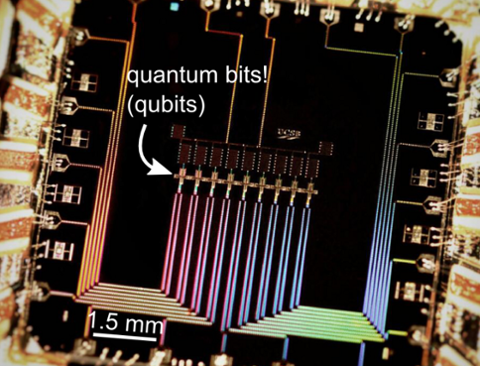
[caption id="attachment_10585" align="aligncenter" width="500"] Visualization of quantum tunneling circuit.[/caption] The powerful, reliable combination of transistors and semiconductors in computer processors could give way to systems built on the way electrons misbehave, all of it contained in circuits that warp even the most basic rules of physics. Rather than relying on a predictable flow of electrons that appear to know whether they are particles or waves, the new approach depends on quantum tunneling, in which electrons given the right incentive can travel faster than light, appear to arrive at a new location before having left the old one, and pass straight through barriers that should be able to hold them back. Quantum tunneling is one of a series of quantum-mechanics-related techniques being developed as possible replacements for transistors embedded in semiconducting materials such as silicon. Unlike traditional transistors, circuits built by creating pathways for electrons to travel across a bed of nanotubes are not limited by any size restriction relevant to current manufacturing methods, require far less power than even the tiniest transistors, and do not give off heat or leak electricity as waste products, according to Yoke Khin Yap of Michigan Technological University, lead author of a paper describing the technique, which was published in the journal Advanced Materials last week. In traditional circuits, transistors are laid down in a bed of silicon that acts as an insulator to prevent crosstalk between circuits. In circuits based on quantum tunneling, silicon is replaced by nanotubes made of boron nitride and electrical pathways consisting of quantum dots—carefully placed bits of gold as small as three nanometers across (PDF). In experiments at Oak Ridge National Laboratory (home of Titan, the supercomputer recently demoted from fastest supercomputer in the world to second-fastest), Yap's team discovered that running the right voltage of current across gold-decorated boron nitride nanotubes allowed electrons to tunnel precisely from one quantum dot to the other, even without the restraining effect of traditional transistor circuits. "Imagine that the nanotubes are a river, with an electrode on each bank. Now imagine some very tiny stepping stones across the river," Yap explained in an announcement accompanying the paper. "The electrons hopped between the gold stepping stones. The stones are so small, you can only get one electron on the stone at a time. Every electron is passing the same way, so the device is always stable." The nanotube substrate is an effective insulator until the right level of current is applied, which allows it to become conductive and open the pathway of quantum dots to a flow of electrons. Turning off the current turns nanotubes back into insulators, halting the flow of electrons and the kind of power leakage between circuits that wastes electricity in traditional transistor circuits (and generates waste heat as well). Researchers at the University of Notre Dame, Pennsylvania State University and elsewhere have also built semi-conductor-free transistor circuits, called tunneling field effect transistors (TFET). In both designs, the electrons tunnel directly through the physical material of the substrate rather than leaping from one quantum dot to another or following a pre-defined channel. "With tunnel transistors, we have a new kind of gate, a gate that the current can flow through instead of over," Alan Seabaugh, engineering researcher at Notre Dame and member of the team that developed TFETs, wrote in a statement. "We adjust the thickness of the gate electrically to turn the current on and off." Until now, TFETs and similar quantum-tunneling designs "only operate at liquid-helium temperatures," rather than room temperature as Yap's design has done, according to John Jaszczak, a Michigan Tech physicist who developed the theoretical framework for Yap's designs. The key to making electrons misbehave in ways consistent enough to be developed into integrated circuits is the nanoscale size of the entire circuit—approximately one micron long and 20 nanometers wide—and of the quantum dots and nanotubes. "The gold islands have to be on the order of nanometers across to control the electrons at room temperature," Jaszczak wrote. "If they are too big, too many electrons can flow," which can waste electricity and undermine circuit stability. BNNT-based nanocircuits are also unlikely to run into the same size barriers that may halt the development of ever-smaller circuit designs based on transistors carved into silicon or other semiconductors. "Theoretically, these tunneling channels can be miniaturized into virtually zero dimension when the distance between electrodes is reduced to a small fraction of a micron," according to Yap. Neither Yap nor Jaszczak have predicted when their nanotube-based circuits could find their way into commercially produced processor designs—but Yap has already filed for an international patent that would allow the technology to be controlled and licensed for commercial development. Image: Yoke Khin Yap
Visualization of quantum tunneling circuit.[/caption] The powerful, reliable combination of transistors and semiconductors in computer processors could give way to systems built on the way electrons misbehave, all of it contained in circuits that warp even the most basic rules of physics. Rather than relying on a predictable flow of electrons that appear to know whether they are particles or waves, the new approach depends on quantum tunneling, in which electrons given the right incentive can travel faster than light, appear to arrive at a new location before having left the old one, and pass straight through barriers that should be able to hold them back. Quantum tunneling is one of a series of quantum-mechanics-related techniques being developed as possible replacements for transistors embedded in semiconducting materials such as silicon. Unlike traditional transistors, circuits built by creating pathways for electrons to travel across a bed of nanotubes are not limited by any size restriction relevant to current manufacturing methods, require far less power than even the tiniest transistors, and do not give off heat or leak electricity as waste products, according to Yoke Khin Yap of Michigan Technological University, lead author of a paper describing the technique, which was published in the journal Advanced Materials last week. In traditional circuits, transistors are laid down in a bed of silicon that acts as an insulator to prevent crosstalk between circuits. In circuits based on quantum tunneling, silicon is replaced by nanotubes made of boron nitride and electrical pathways consisting of quantum dots—carefully placed bits of gold as small as three nanometers across (PDF). In experiments at Oak Ridge National Laboratory (home of Titan, the supercomputer recently demoted from fastest supercomputer in the world to second-fastest), Yap's team discovered that running the right voltage of current across gold-decorated boron nitride nanotubes allowed electrons to tunnel precisely from one quantum dot to the other, even without the restraining effect of traditional transistor circuits. "Imagine that the nanotubes are a river, with an electrode on each bank. Now imagine some very tiny stepping stones across the river," Yap explained in an announcement accompanying the paper. "The electrons hopped between the gold stepping stones. The stones are so small, you can only get one electron on the stone at a time. Every electron is passing the same way, so the device is always stable." The nanotube substrate is an effective insulator until the right level of current is applied, which allows it to become conductive and open the pathway of quantum dots to a flow of electrons. Turning off the current turns nanotubes back into insulators, halting the flow of electrons and the kind of power leakage between circuits that wastes electricity in traditional transistor circuits (and generates waste heat as well). Researchers at the University of Notre Dame, Pennsylvania State University and elsewhere have also built semi-conductor-free transistor circuits, called tunneling field effect transistors (TFET). In both designs, the electrons tunnel directly through the physical material of the substrate rather than leaping from one quantum dot to another or following a pre-defined channel. "With tunnel transistors, we have a new kind of gate, a gate that the current can flow through instead of over," Alan Seabaugh, engineering researcher at Notre Dame and member of the team that developed TFETs, wrote in a statement. "We adjust the thickness of the gate electrically to turn the current on and off." Until now, TFETs and similar quantum-tunneling designs "only operate at liquid-helium temperatures," rather than room temperature as Yap's design has done, according to John Jaszczak, a Michigan Tech physicist who developed the theoretical framework for Yap's designs. The key to making electrons misbehave in ways consistent enough to be developed into integrated circuits is the nanoscale size of the entire circuit—approximately one micron long and 20 nanometers wide—and of the quantum dots and nanotubes. "The gold islands have to be on the order of nanometers across to control the electrons at room temperature," Jaszczak wrote. "If they are too big, too many electrons can flow," which can waste electricity and undermine circuit stability. BNNT-based nanocircuits are also unlikely to run into the same size barriers that may halt the development of ever-smaller circuit designs based on transistors carved into silicon or other semiconductors. "Theoretically, these tunneling channels can be miniaturized into virtually zero dimension when the distance between electrodes is reduced to a small fraction of a micron," according to Yap. Neither Yap nor Jaszczak have predicted when their nanotube-based circuits could find their way into commercially produced processor designs—but Yap has already filed for an international patent that would allow the technology to be controlled and licensed for commercial development. Image: Yoke Khin Yap