 IBM's POWER 7+ performance.[/caption] This week, vendors including IBM, Fujitsu, and Oracle offered a look at the chips that drive their big-iron workloads. At the Hot Chips conference, which ran Aug. 27-29 in Cupertino, Calif., IBM discussed its Power 7+ architecture as well as the z12, the chip that debuted inside the new IBM zEnterprise mainframe that debuted this week. Fujitsu and Oracle, for their part, presented their own spins on the rival SPARC architecture. One of the more ambitious approaches to chip architecture was the AMCC X-Gene, an attempt to push ARM into at least a small portion of the data center. Other vendors took a more traditional approach, largely sacrificing power for raw performance. (We've purposely excluded the Intel Xeon E5 family, only because the family, code-named "Romley," was formally launched in March and is therefore well-known.)
Server Chips Spotlighted at Hot Chips
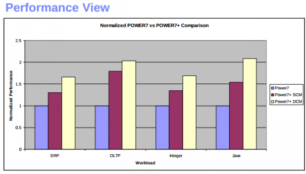
[caption id="attachment_4089" align="aligncenter" width="618"]  IBM's POWER 7+ performance.[/caption] This week, vendors including IBM, Fujitsu, and Oracle offered a look at the chips that drive their big-iron workloads. At the Hot Chips conference, which ran Aug. 27-29 in Cupertino, Calif., IBM discussed its Power 7+ architecture as well as the z12, the chip that debuted inside the new IBM zEnterprise mainframe that debuted this week. Fujitsu and Oracle, for their part, presented their own spins on the rival SPARC architecture. One of the more ambitious approaches to chip architecture was the AMCC X-Gene, an attempt to push ARM into at least a small portion of the data center. Other vendors took a more traditional approach, largely sacrificing power for raw performance. (We've purposely excluded the Intel Xeon E5 family, only because the family, code-named "Romley," was formally launched in March and is therefore well-known.)
 IBM's POWER 7+ performance.[/caption] This week, vendors including IBM, Fujitsu, and Oracle offered a look at the chips that drive their big-iron workloads. At the Hot Chips conference, which ran Aug. 27-29 in Cupertino, Calif., IBM discussed its Power 7+ architecture as well as the z12, the chip that debuted inside the new IBM zEnterprise mainframe that debuted this week. Fujitsu and Oracle, for their part, presented their own spins on the rival SPARC architecture. One of the more ambitious approaches to chip architecture was the AMCC X-Gene, an attempt to push ARM into at least a small portion of the data center. Other vendors took a more traditional approach, largely sacrificing power for raw performance. (We've purposely excluded the Intel Xeon E5 family, only because the family, code-named "Romley," was formally launched in March and is therefore well-known.)